A Time Scaling Theory for Multi-Layer Electronic Systems
Author: Tingbo He (Huawei Semiconductor) | Leading LogicFolding from theory to mass production
ISCAS 2026 live announcement: Huawei Board Director & President of Semiconductor Business, Tingbo He, officially introduces the "Tau (τ) Law".
The Kirin mobile chip launching this fall will be the first to adopt LogicFolding technology, delivering substantial performance gains.
He’s paper "A Time Scaling Theory for Multi-Layer Electronic Systems" was submitted today to the ChinaXiv preprint platform, detailing the τ Law and outlining Huawei’s future chip development roadmap.
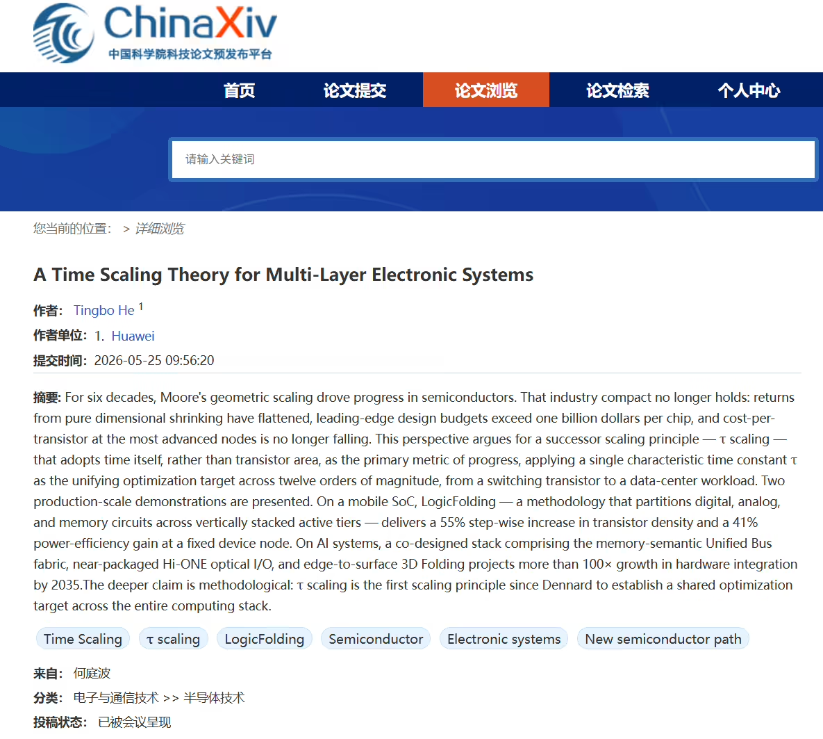
He argues that the pure "geometric era" of the chip industry has ended.
Moore’s Law only addresses the time dimension (transistor count doubling every 18–24 months), and the era of per-layer independent optimization is also over.
The first production‑scale test of the τ Law is carried out on mobile devices.
A smartphone SoC is a rare case where a single chip constitutes the whole system: multi‑socket parallelism is unavailable, no thousand‑node architecture can hide slow connections, and total power is only a few watts under thermal constraints.
After 2020, when access to advanced nodes became restricted, the practical problem became: with a fixed process node, how to deliver generation‑over‑generation performance improvements on a single chip?
The answer that emerged is LogicFolding.
LogicFolding is a design methodology that partitions digital, analog, and memory circuits into vertically stacked active layers, jointly optimizing performance, power, and area according to time‑scaling principles.
Kirin 2026 silicon results:
- Transistor density stepped from 155 MTr/mm² to 238 MTr/mm² in a single generation — an improvement that previously required three years of geometric scaling.
- SoC performance core energy efficiency improved by 41%, and maximum clock frequency rose by nearly 13% to 3.1GHz.
- High‑speed global Network‑on-Chip (NoC) data paths reduced area by 55% and improved power delivery stability.
- Post‑silicon clock skew adjustment contributed >5% additional SoC performance.
- For SRAM — where access speed, energy/bit, and area heavily depend on bit‑line and word‑line length — LogicFolding shortens critical paths, reduces energy/bit, and raises operating frequency by over 40%.
- On a typical processing core, dual‑layer folding reduces clock buffer count by >50%, lowers clock skew by 25%, and cuts routing length by about 30%.
These gains are achieved on a fixed device node, not through new lithography steps, but through topological reorganisation of logic in three dimensions.
The LogicFolding implemented in Kirin 2026 is deliberately conservative: hybrid bonding pitch is 1.5μm, and folding is applied selectively only to critical paths, not across the entire design.
Over the next decade, LogicFolding will evolve from local critical‑path folding to full‑scale multi‑layer folding — three, four, or more active layers per package.
From 2026 to 2035, transistor density is expected to reach 400 MTr/mm² or higher.
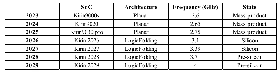
At the same time, LogicFolding paves the way for CPU core frequencies to reach 4 GHz and beyond.
The roadmap is both technically feasible and economically viable.
Kirin chip naming: the paper shows Kirin 2026, 2027, 2028, 2029.
Kirin 2027 is already marked as "Silicon" (substantial progress), while Kirin 2028/2029 are in pre‑silicon phase.
For AI accelerators: Ascend 910C, 950, and by 2030 Ascend 990 will also introduce LogicFolding, with hardware integration expected to exceed 100× by 2035.
The Unified Bus adopts a single memory‑semantic protocol, cutting end‑to‑end remote access latency to ~100ns (a 500× improvement).
The Hi‑ONE optical engine delivers 8Tb/s per module, dramatically reducing power and complexity.
3D folding resolves the fan‑out dilemma by moving storage and optical I/O from the periphery to vertical surfaces, enabling N² scaling for all resources and restoring area‑derived benefits.
Kirin roadmap (data from paper)
| Chip | Status | LogicFolding generation | Expected density/frequency |
|---|---|---|---|
| Kirin 2026 | Mass production | Conservative (local critical paths) | 238 MTr/mm², 3.1GHz, +41% efficiency |
| Kirin 2027 | Silicon (taped out) | Enhanced folding | Higher density/frequency |
| Kirin 2028 | Pre‑silicon | Multi‑layer folding (3 layers) | towards 3.6GHz+ |
| Kirin 2029 | Pre‑silicon | Full‑scale folding | target 4GHz+ |
Ascend AI accelerators will adopt LogicFolding around 2030; Ascend 990 will drive >100× hardware integration gain (compared to 2026 baseline).
The paper also highlights open challenges: need for 3D‑native EDA tools, wafer‑to‑wafer process variation compensation, vertical interconnect RC tradeoffs, and energy‑companion design.
τ scaling provides a fresh benchmarking framework to guide post‑Moore investment.
Paper link: https://chinaxiv.org/abs/202605.00224 (open access preprint)


💬 Technical discussion · selected comments
⌨️ From semiconductor engineer & architect community · hot discussion at ISCAS 2026